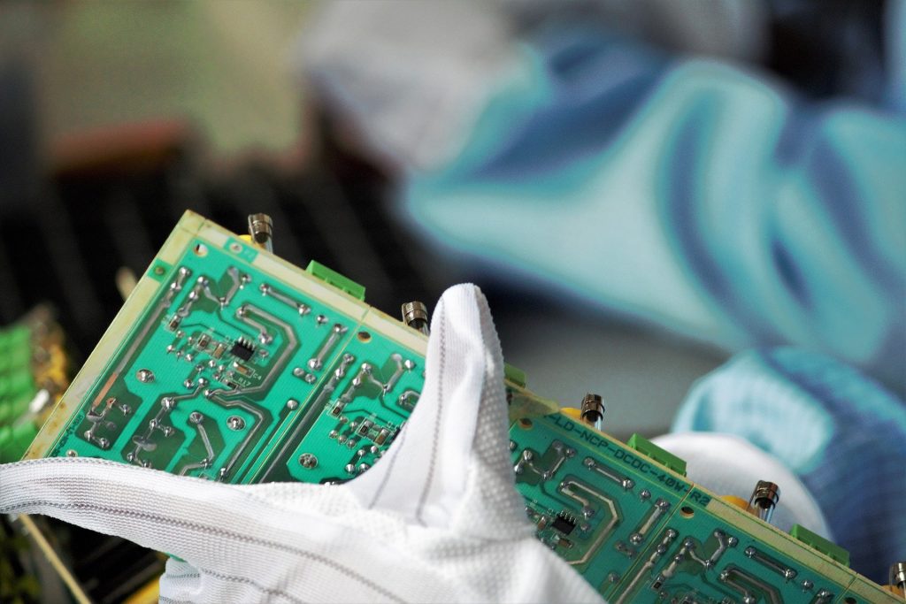
In the PCB industry, many changes are happening every day due to new technologies and innovative thinking. As a result, a PCB producer or PCB assembly service provider should keep abreast with these changing times and emerging challenges by implementing advanced tools and techniques. These tools and techniques are integrated into a PCB Inspection Process that helps the company detect as early as possible any imperfections in the PCB material. Doing so can prevent costly mistakes in the long run. PCB Inspection is becoming an essential part of the entire PCB process, which is a crucial step in determining the quality of the final product. To prevent these, PCB producers and PCB assembly service providers perform different kinds of internal inspections on PCBs at various stages of production.
A visual inspection is done to detect any blemishes and defects in the PCB. The visual inspection procedure is usually done on the PCB top surface to easily be seen and detected. For this, special light with a high-intensity level (often called the “light eye” technique) is used, and as a result, defects are easily spotted and detected on the PCB.
Another common inspection technique that is widely used is the electrical discharge spraying (EDS) inspections. This inspection method involves spraying the areas with a high concentration of tincture of organic solvents to check for the existence of copper traces and traces of lead, mercury, and many other hazardous chemicals, as well as corrosion. The main PCB inspection technique, which is widely used, is thermal conductivity detection (TDS). Through this method, the quality of the PCB can be easily determined.
By far, the most widely used testing methods are the self-verifying and functional testing methods. The self-verifying inspection technique refers to the PCB alignment testing, which ensures that the PCB is not aligned incorrectly. The functional testing technique is mainly adopted for electrical components, mechanical components, and graphical designs.
PCBs manufactured with the help of fiber optic techniques are often subjected to the third type of inspection process. Fiber optic inspection helps detect the presence of discontinuous spots surrounded by a layer of black plastic. These spots are usually the result of the friction that is caused due to the contact between the PCB material and the various metals used during its manufacturing. Through the microscope, it is possible to inspect the internal junctions of the PCBS’s with the help of appropriate tools. However, before going in for such inspection procedures, many guidelines need to be considered.


")


