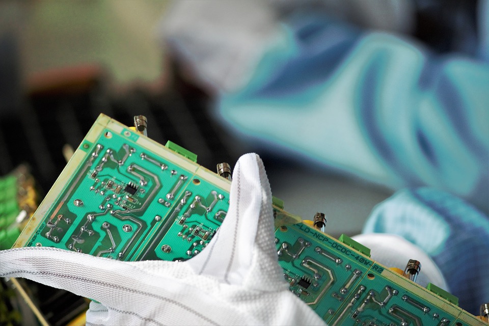
A prototype circuit board is a bare “bones” board with no components soldered on and no solder mask of any kind. All the holes in the board are drilled and plated, and ready to accept component pins. A proper PCB design will have all necessary information on it that allows for easy soldering and assembly.
What Prototype Circuits Boards Are For
The main use for a prototype circuit board is to allow the designer/engineer of particular electronic devices or products to see if their design works. Sometimes engineers will make drawings and schematics of what they want the finished circuit board to look like (although this is not as common) and then make a prototype board to see if those designs will work.
How Prototype PCBs Are Different from Finished PCBs
In a finished PCB, the holes have been drilled and plated, but they do not have any other important features, such as a solder mask or silkscreen. In a prototyping circuit board, the pads are also the same as those on the finished board, and they are often very close to each other in size. The only thing that separates the pads is a bit of a solder mask. This allows components to be placed on the circuit board without any confusion about where they should go (this is especially important if you use surface mount technology).
How Prototype Circuit Boards Are Made
The process of making prototype circuit boards depends on the size and shape of the board you want to make. For example, if you wanted to create a prototyping circuit board with 16 holes, each with its pads, it would be made by creating a “mask” that has all 16 drillings in place (this is done in photoresist). Then the holes are drilled in the board with a slightly smaller bit than what you would want to use when making the finished product.
After this, all of the pads on the circuit board will be plated in copper (just like they would be in unfinished circuit boards), but in this case, because the holes are smaller than what you would want for finished boards, there will be no solder mask.
After this process is completed, the board should have all the necessary information to place components easily. The next step is to create a solder stencil that will allow surface mount components to be easily soldered onto the circuit board.
The last step is to put solder paste on the pads of the board, place all necessary surface mount components onto their respective pad locations, and then “flash” or bake everything into place. Finally, you have a fully functioning prototyping PCB that can be used for testing purposes. To be used in a finished product, you would have to add a solder mask and silkscreen.
Properly using a prototype circuit board is important because it allows for quick testing of whether or not your design will work before you spend any time completing the soldering process. In addition, if something should go wrong with your PCB during testing, you can correct the problem quickly and avoid wasting more time on it.
